Microwave Office łnĹéľŢ§@¨ĎĄÎ»ˇ©ú
![]()
ˇ@
°ňĄ»ŔôąŇ¤¶˛ĐˇG
step1ˇG¶}±Ň Microwave ¤§«áŞşµřµˇ
setp2ˇG«ŘĄß¤@Ó·sŞşproject
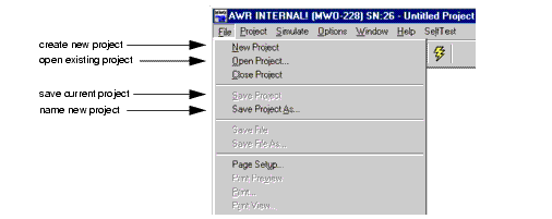
step3ˇG«ŘĄß¤@Ó·sŞşąq¸ôŔɡG
ˇ@
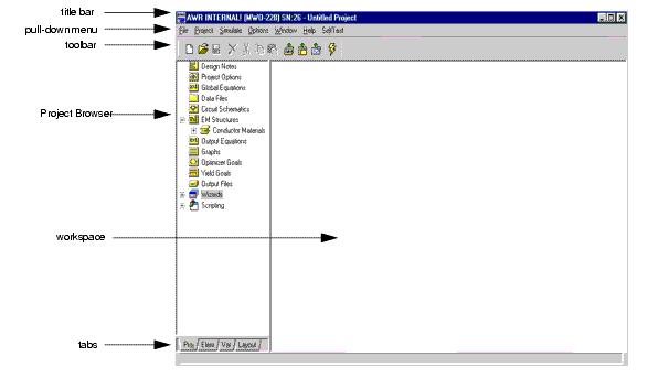
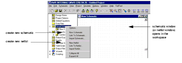
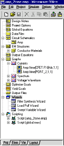
Project BrowserˇG¦p¤UąĎ©ŇĄÜ
|
Object
|
Description
|
|---|---|
|
Design Notes
|
Displays a simple text editor in which you can make notes.
|
|
Project Frequency
ˇ@ |
Allows you to specify a default range of frequencies to be used for any
linear, nonlinear, or EM simulations performed for this project.
For more information, see
"Configuring Global Project Frequency" .
|
|
Global Equations
ˇ@ |
Allows you to define equations and/or functions to be used as parameter
values in schematics created within this project.
For more information, see Chapter 11.
|
|
Data Files
ˇ@ |
Allows you to import data files to be used as subcircuits in schematics
created within this project. The imported data files display as
subobjects of Data Files. Data files imported for use as subcircuits can
be Touchstone format or raw data files.
Also allows you to import data files to be used for performance
comparison purposes. The imported data files display as subobjects of
Data Files. Data files imported for comparison purposes can be DC-IV
format or raw data files. (DC-IV is a Microwave Office format for
reading DC-IV curves that measure a transistor or diode.)
For more information, see
"Importing Data Files Into a Project" .
|
|
Schematics
ˇ@ |
Allows you to create schematics and netlists within this project. These
schematics and netlists display as subobjects of Schematics. Also
contains the Default Ckt Options subobject, which allows you to specify
schematic display, simulation, and layout options that apply to all
schematics within this project.
For more information, see Chapters 2 and 3.
|
|
EM Structures
ˇ@ |
Allows you to create EM structures within this project. These structures
display as subobjects of EM Structures. Also contains the Default EM
Options subobject, which allows you to specify drawing and simulation
options that apply to all EM structures within this project.
For more information, see Chapter 4.
|
|
Conductor Materials
ˇ@ |
Allows you to define conductor materials to characterize the loss
associated with the planar conductors of EM structures within this
project. The materials display as subobjects of Conductor Materials.
This object always contains the Perfect Conductor subobject -- a perfect
conductor is the default conductor material.
For more information, see
"Conductor Materials" .
|
|
Output Equations
ˇ@ |
Allows you to specify equations used to post-process measurement data
prior to displaying it in tabular or graphical form.
For more information, see
"Output Files" .
|
|
Graphs
ˇ@ |
Allows you to create graphs to display the output of simulations
performed within this project. The graphs display as subobjects of
Graphs. You can create the following graphs types: rectangular, Smith
Chart, polar, histogram, antenna plot, tabular, and constellation.
For more information, see Chapter 5.
|
|
Optimization Goals
ˇ@ |
Allows you to specify optimization goals for this project. The goals
display as subobjects of Optimization Goals.
For more information, see Chapter 8.
|
|
Yield Goals
ˇ@ |
Allows you to specify yield goals for this project. The goals display as
subobjects of Yield Goals.
For more information, see Chapter 8.
|
|
Output Files
ˇ@ |
Allows you to specify output files to contain the output of simulations
performed within this project, as an alternative to graphical output.
The output files display as subobjects of Output Files. Output files can
be Touchstone format (S, Y, or Z-parameters) (for circuit and EM
simulations), SPICE Extraction files (for EM simulations), AM to AM or
AM to PM files (for nonlinear circuit simulations), or spectrum data
files (for nonlinear circuit simulations).
For more information, see
"Output Files" .
|
|
Scripts
|
Allows you to create scripts to automate tasks within Microwave Office.
The scripts display as subobjects of Scripts.
For more information, see
"Script Development Environment" .
|
|
Wizards
|
Allows you to add externally-authored wizards as add-on tools to
Microwave Office. The wizards display as subobjects of Wizards.
For more information, see
"Microwave Office Design Wizards" .
|
step4ˇGhelpŞş¤čŞk§A¤@©wn·|
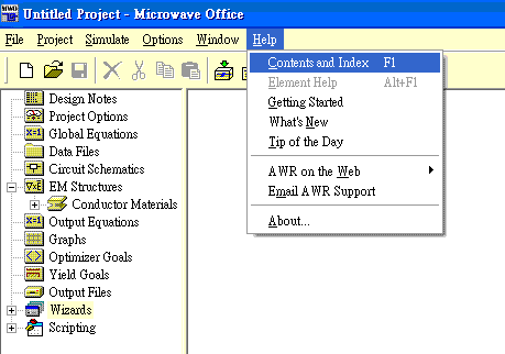
Microwave Office Help pages provide information as you need it on the windows, menu choices, and dialog boxes that compose the design environment, as well as on the concepts involved.
To access Help, choose Help from the Microwave Office pull-down menu, or press the F1 key anytime you are using Microwave Office to display the Help menu. The Help menu includes the following choices:
|
Menu Choice
|
Description
|
|---|---|
|
Contents and Index
|
See Help organized by subject, find important topics from an index, or
perform a search for any character string in the Help text.
|
|
Element Help
|
Access help specifically on the electrical elements that compose the
Element Browser.
|
|
Getting Started
|
View on-line versions of this guide and other Microwave Office
documentation.
|
|
Interactive Tutorials
|
Run tutorials that help you learn how to perform various tasks within the
Microwave Office environment. These are the same tutorials as on the
Tutorial Disk.
|
|
Tip of the Day
|
Get useful tips on using Microwave Office.
|
|
AWR on the Web
|
Launch the Applied Wave Research website.
|
|
Report Problem
|
Report a problem to Applied Wave Research technical support via e-mail.
|
![]()
ˇ@
ĄH²łćŞşˇiLPˇjąę¨Ň¨Ó»ˇ©ú¬yµ{ˇG
ˇ@
This example demonstrates how to use Microwave Office to simulate a basic lumped element filter using the linear simulator. It includes the following main steps:
ˇ@
| ˇ@ |
|
Creating a schematic ˇ@ |
| ˇ@ |
|
Adding graphs and measurements ˇ@ |
| ˇ@ |
|
|
| ˇ@ |
|
Tuning the circuit ˇi§Ú̳̥DnnĄÎŞşˇj ˇ@ |
|
|
Creating variables ˇ@ |
|
|
|
Optimizing the circuit ˇ@ |
ˇ@
¨BĆJ¦p¤UˇG
To create a new project,
|
1
|
Choose
File > New Project from the pull-down menu.
|
|
2
|
Choose
File > Save Project As from the pull-down menu. The Save As
dialog box appears.
|
|
3
|
Type a project name (for example, "linear_example"),
and click
Save.
|
ˇ@
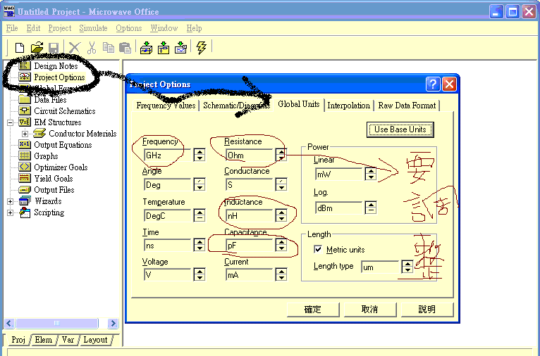
To set default project units,
|
1
ˇ@ |
Choose
Options > Project Options from the pull-down menu. TheProject
Options dialog box appears.
|
|
2
|
Click the
Global Units tab.
ˇ@ |
|
3
ˇ@ |
Modify the units by clicking the arrows to the right of the field so
that they match those in the figure below, and click
OK.
|
ˇ@
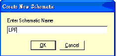
To create a schematic,
|
1
ˇ@ |
Choose
Project > Add Schematic > New Schematic from the pull-down menu.
The Create New Schematic dialog box appears.
|
|
2
ˇ@ |
Type "lpf",
and click
OK. A schematic window displays in the workspace and the
schematic appears as a subgroup of the
Circuit Schematics node in the Project Browser.
|
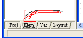
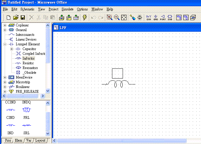
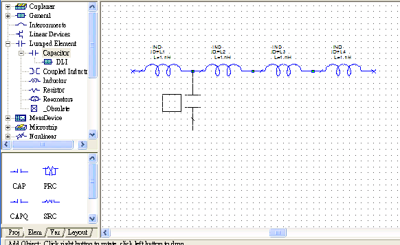
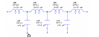
To place elements in a schematic,
|
1
ˇ@ |
Click the
Elem tab in the lower left of the window to display the Element
Browser.
|
|
2
ˇ@ |
Expand the Lumped Element group by clicking the
+ symbol to the left of the group.
|
|
3
ˇ@ |
Click on the
Inductor subgroup of the Lumped Element node in the Element
Browser. A set of inductor models displays in the lower pane.
|
|
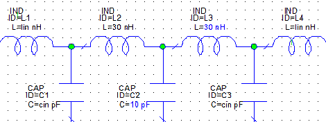
4
ˇ@ |
Click on the
IND model, and holding the mouse button down, drag it into the
schematic, release the mouse button, position the element as shown in
the figure below, and click to place it.
|
|
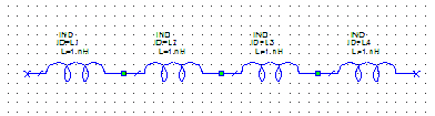
5
ˇ@ |
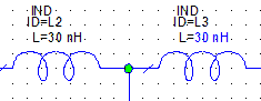
Repeat Step 4 three times, aligning
and connecting each inductor as shown below.
|
|
6
ˇ@ |
Now click on the
Capacitor subgroup of the Lumped Element node in the Element
Browser. A set of capacitor models displays in the lower pane.
|
|
7
ˇ@ |
Click on the
CAP model, and holding the mouse button down, drag it into the
schematic, release the mouse button, right-click to rotate the element,
position it as shown in the figure below, and click to place it.
|
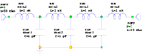
ąĎĄÜ¦p¤U
|
ˇ@ |
żé¤J·sąq¸ôŞşŔɦW |
|
ˇ@ |
żďľÜło¸Ě |
| ˇ@
ˇ@ |
żď¨úąq·P©ń¸m©óąq¸ôąĎ¤W |
| ˇ@
ˇ@ |
łsÄň©ń¸mĄ|Óąq·P |
| ˇ@
ˇ@ |
©ń¸mąq®eˇAĄtĄ~§AĄiĄHµo˛{ąq®eŞşÂ\©ńˇA ¤w¸g¤Ł¬OĄ¦ć¤č¦VˇAło¬O¦b©Ô¦˛ŞşąLµ{¤¤ ľA®ÉŞş«ö¤U·Ćą«ĄkÁäˇA§YĄiÂŕ´«90«×ˇA¨â ¤UŞş¸ÜˇA«h±N180«×ŞşÂŕ´«ˇI |
| ˇ@
ˇ@ |
łsÄň¤TÓąq®e |
  |
±N˝u¸ôłs±µ°_¨ÓˇG «Ü²łćˇA§AĄun§â·Ćą«˛ľ¦Ü¸ÓÂI¤W¤čˇAÂI ¤@¤UĄŞÁäˇA¦A¨ě˛×ÂIÂI¤@¤UĄkÁä§YĄiˇC |
| ˇ@
ˇ@ |
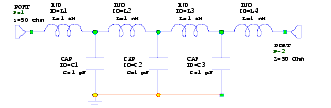
¦b¤u¨ă¦CŞş¤W¤čˇA¬Ý¨Ł¤F¶ÜˇH ¦ł¤@ÓĽg GND ĄH¤Î PORT Şş¶ÜˇH Ş˝±µÂI¤@¤U¤pąĎĄÜˇAµM«á©ą¤U©Ô§YĄiˇC |
ˇ@
|
1
ˇ@ |
Double-click on the Ind L1 graphic in the schematic window. The Element
Options dialog box appears.
|
|
2
ˇ@ |
Click on the value text box in the Inductance (L) row, enter "15"
in the Value field, and click
OK. The change is reflected in the schematic.
|
|
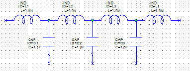
3
ˇ@ |
Follow Steps 1 and 2 to edit the inductor and capacitor values to match
what is shown below. (To edit capacitor values, select
C in the Parameters list box.)
|
¦p¤UąĎ©ŇĄÜ
|
1
ˇ@ |
Click the
Proj tab in the lower left of the window to activate the Project
Browser.
|
|
2
ˇ@ |
Double-click on the
Project Options group. The
Project Options dialog box appears.
|
|
3
ˇ@ |
Click on the
Frequency Values tab.
|
|
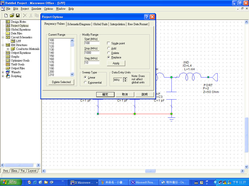
4
ˇ@ |
Type "100"
in the Start field, type "1000"
in the Stop field, and type "10"
in the Step field. Click
Apply. The Current Range scroll box displays the frequency range
and steps you have just specified.
|
|
5
ˇ@ |
Click
OK.
|
ˇ@
ˇ@
 ˇ@ |
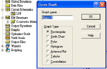
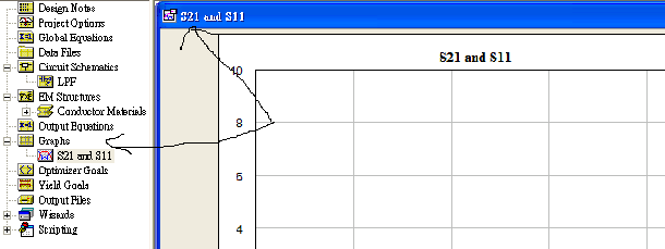
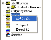
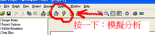
Right-click on the Graphs group in the Project Browser, and choose Add Graph from the pop-up menu. The Create Graph dialog box appears. |
| ˇ@
ˇ@ |
żďľÜ§A·Qn¬ÝŞşąĎ§ÎˇA¨ä¤¤¦ł¨âÓ¬O¤ń¸ű ±`¨ĎĄÎŞşˇA¨äĄLŞşżď¶µˇA«h¤ń¸ű¤ÖĄÎˇA¤@Żën¬Ý¤Ń˝ułő«¬Şş¸ÜˇA¤Ł·|¨ĎĄÎło¤@ÓłnĹéˇAŞ˝±µĄÎIE3D©ÎHFSS¨Ó¬ÝˇC Żx§ÎąĎˇGˇi¤@ŻëĄHdBȨӬݡj Ąv±K´µąĎˇGˇiĄiĄH¬ÝmatchŞş±ˇ§Îˇj |
| ˇ@
|
Type "s21 and s11" in Graph Name. Select the Rectangular radio button for Graph Type, and click OK. The graph displays in a window in the workspace and appears as a subgroup of the Graphs node in the Project Browser |
|
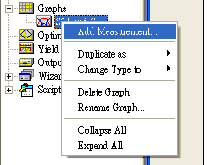
1
ˇ@ |
Right-click on the
s21 and s11 subgroup in the Project Browser, and choose
Add Measurement from the pop-up menu. The Add Measurement dialog
box appears.
|
|
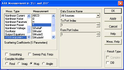
2
|
Select
S in the Measurement scroll box. Select
lpf in the Data Source Name field by clicking on the arrow to the
right of the field. Select the value "1"
in both the To Port Index and From Port Index fields by clicking on the
arrows to the right of the fields. Check the
DB checkbox and select the
Mag. radio button. Click
Apply.
|
|
3
ˇ@ |
Change the value in the To Port Index fields to "2",
and click
Apply.
|
|
4
ˇ@ |
Click
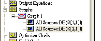
OK. The measurements lpf:DB(|S[1,1]|) and lpf:DB(|S[2,1]|) appear
as subgroups of the s21 and s11 group in the Project Browser.
|
ˇ@
ˇ@
ˇ@
ˇ@
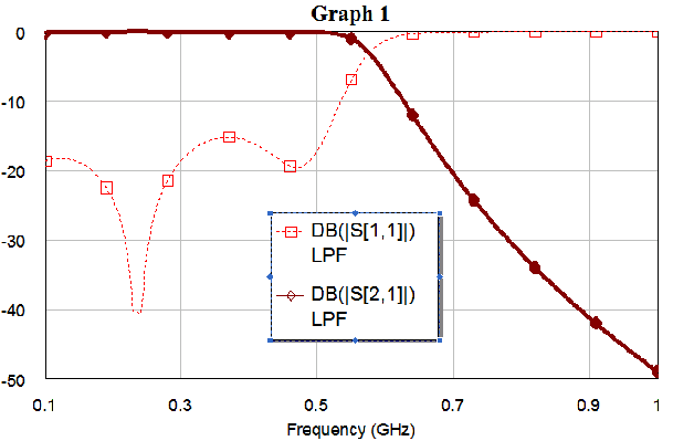
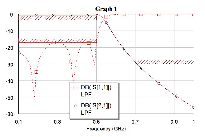
°ő¦ć¤ŔŞR»P°ő¦ćµ˛ŞGˇG
ˇ@
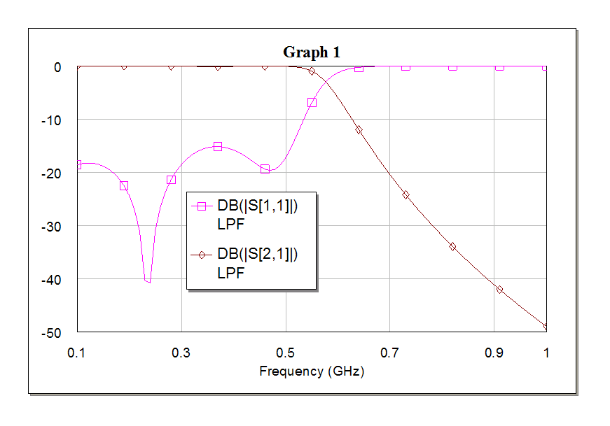
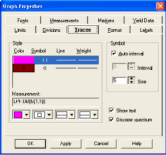
¦b¤WąĎ¤¤ˇAĄi¦bąĎ¤W«ö¤@¤U·Ćą«ĄkÁäˇA§YĄi§ďĹܹϪşĂC¦â©Î˛Ę˛ÓµĄ°ŃĽĆˇI»PEXCELŞşąĎŞíĄ\Żŕ¬Ű¦üˇC
ˇ@
¦]¬°Ą¦ŞşąĎ¬Ý°_¨ÓˇA¤ń¸ű¦n¬ÝˇI
©ŇĄH¤@Żë¤HłŁ¬O±N¨äĄLĽŇŔŔłnĹé°ő¦ć«áŞş S°ŃĽĆ©ń¸m¦ąąĎŞí¨Ó¬Ý
ĄH«K©ó§@łř§iˇI
ˇ@
ˇ@
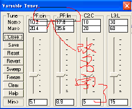
Tune the circuit
|
1
ˇ@ |
Click on the schematic window to make it active.
|
|
2
ˇ@ |
Click the
Tune Tool icon in the toolbar.
|
|
3
ˇ@ |
Move the cursor over the L parameter of IND L1. The cursor displays as a
cross
|
|
4
ˇ@ |
Click the mouse button to activate the L parameter for tuning. The
parameter appears in an alternate color.
|
|
5
ˇ@ |
Repeat Steps 2 through 4 for elements CAP C1, CAP C3, and IND L4.
|
|
6
ˇ@ |
Click on the graph window to make it active.
|
|
7
ˇ@ |
Choose
Simulate > Tune from the pull-down menu. The Variable Tuner
dialog box appears.
|
|
8
ˇ@ |
Click on a tuning button, and holding the mouse button down, slide the
tuning bar up and down. Observe the simulation change on the graph as
the variables are tuned.
|
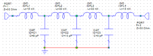
|
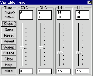
9
ˇ@ |
Slide the tuners to the values shown below, and observe the resulting
response on the graph of the tuned circuit.
|
![]()
ˇ@
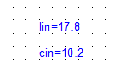
Filters are typically symmetric circuits. To optimize the circuit, we must change some of the parameter values to variables.
ˇ@
|
1
ˇ@ |
Click on the schematic window to make it active.
|
|
2
ˇ@ |
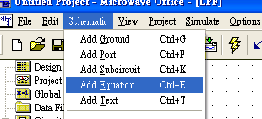
Choose
Schematic > Add Equation from the pull-down menu.
|
|
3
ˇ@ |
Move the mouse cursor into the schematic. An edit box appears.
|
|
4
ˇ@ |
Position the edit window in the top area of the schematic window, and
click to place it.
|
|
5
ˇ@ |
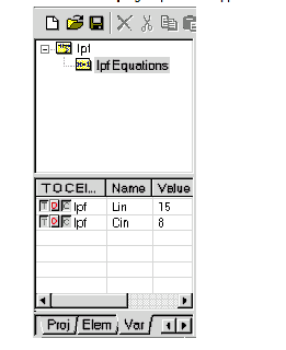
Type "Lin=15"
in the edit box, and click the mouse outside of the edit box.
|
|
6
ˇ@ |
Repeat Steps 2 through 5 to create a second edit box, but type "Cin=8",
and click the mouse outside of the edit box.
|
|
7
ˇ@ |
Double-click on the
L parameter value of IND L1. An edit box appears. Type the value
"Lin".
|
|
8
ˇ@ |
Repeat Step 7 to change the L parameter of IND L4 to "Lin",
and the C parameters of CAP C1 and CAP C3 to "Cin",
as shown in the figure below.
|
|
9
ˇ@ |
Click the
Var tab in the lower left of the window.
|
|
10
ˇ@ |
Click on the
+ symbol to expand the lpf group.
|
|
11
ˇ@ |
Click on
lpf Equations. The lower window displays variables Cin and Lin.
|
|
12
ˇ@ |
Click the
O checkbox for both variables.
|
|
13
ˇ@ |
Click the
lpf group in the upper window, and click the
O checkbox corresponding to C2.
|
ˇ@
ˇ@
ˇ@
ˇ@
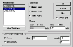
Add Optimization Goals
|
1
ˇ@ |
Click the
Proj tab.
|
|
2
ˇ@ |
Right-click on
Optimization Goals, and choose
Add Opt Goal from the pop-up menu. The New Optimization Goal
dialog box appears.
|
|
3
ˇ@ |
Highlight
lpf:DB(|S[1,1]) in the Measurement list
box. Select the
Meas < Goal radio button in the Goal Type
field, uncheck the
Max checkbox in the Range field, type "500"
in the Stop field, type
-17 in the Goal field, and click
OK.
|
|
4
ˇ@ |
epeat Steps 2 Rand 3, but highlight
lpf:DB(|S[2,1]) in the Measurement list
box, select the
Meas > Goal radio button, uncheck the
Max checkbox, type "500"
in the Stop field, type "-1"
in the Goal field, and click
OK.
|
|
5
ˇ@ |
Repeat Steps 2 and 3 again, but highlight
lpf:DB(|S[2,1]) in the Measurement list
box, select the
Meas < Goal radio button, uncheck
Min, type "700"
in the Start field, type "-30"
in the Goal field, and click
OK.
|
ˇ@
|
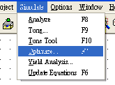
1
ˇ@ |
Choose
Simulate > Optimize from the pull-down menu. The Optimize dialog
box appears.
|
|
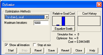
2
ˇ@ |
Select
Random (Local) in the Optimization Methods field by clicking on
the arrow to the right of the field, type "5000"
in the Maximum Iterations field, and click
Start. The simulation runs.
|
|
3
ˇ@ |
When the simulation is complete, click
Close to exit the Optimize dialog box. View the finalized
optimized response in the schematic and on the graph, as shown below.
|
ˇ@
ˇ@
ąF¨ěąw©wŞşĄŘĽĐˇG
ˇ@
ˇ@
ˇ@
ˇ@
ˇ@
ˇ@
ˇ@
ˇ@
ˇ@